Lab4: Seven Segment Display#
Time Estimate2-4 Hours Grade Impact2.5% DueSep 30 @ 3pm Required for Pass
Objective
Implement a simple combinational circuit.
Warning
Before starting any lab, always read the entire lab description. You are working with expensive, fragile hardware. Look particularly closely at these boxes, which warn you of potential problems.
Before the Lab#
Repository#
Accept the invitation to this lab assignment’s Github repository on Canvas.
Equipment#
Please bring the following equipment to this lab:
- Digilent Basys 3 FPGA board
- Compatible (power-and-data) USB cable
- Note taking mechanism (laptop, notebook, etc.)
Pre-Lab Work#
This lab has pre-lab work, specified below. Pre-lab work is due within the first 30 minutes of the lab session designated for this lab (that is, 3:00pm on September 23).
Pre-Lab#
A combinational circuit is a fundamental type of digital electronic circuit whose output is determined solely by its current input values. For Lab 3 and 4, you will design and implement a circuit that controls the 7-segment display on your FPGA board based on the input values from the board’s switches. You’ll try a few approaches to this during these labs.
Minimal Expressions#
Recall the 7-segment encoding, which we can represent with variables $x_3$, $x_2$, $x_1$, $x_0$. Let’s just stick to the first 10 digits for this lab.
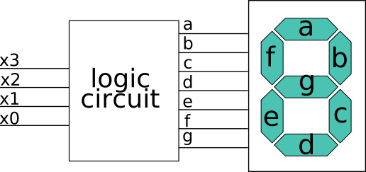
Before the lab, use the truth table you completed for the previous lab to generate simplified expressions for each segment. You may use SoP or PoS form to complete your analysis.
For example, take a look at the truth table for signal a:
| $x_3$ | $x_2$ | $x_1$ | $x_0$ | Digit | a |
|---|---|---|---|---|---|
| 0 | 0 | 0 | 0 | 0 | 1 |
| 0 | 0 | 0 | 1 | 1 | 0 |
| 0 | 0 | 1 | 0 | 2 | 1 |
| 0 | 0 | 1 | 1 | 3 | 1 |
| 0 | 1 | 0 | 0 | 4 | 0 |
| 0 | 1 | 0 | 1 | 5 | 1 |
| 0 | 1 | 1 | 0 | 6 | 1 |
| 0 | 1 | 1 | 1 | 7 | 1 |
| 1 | 0 | 0 | 0 | 8 | 1 |
| 1 | 0 | 0 | 1 | 9 | 1 |
Only two positions have zeroes, so we should use the PoS form.
$$ \begin{gather} \text{a} & = (x_3 + x_2 + x_1 + \overline{x}_0)(x_3 + \overline{x}_2 + x_1 + x_0) && \newline & = ((x_3 + x_1) + x_2 + \overline{x}_0)((x_3 + x_1) + \overline{x}_2 + x_0) &&\text{10b} \newline & = (x_3 + x_1) + (x_2 + \overline{x}_0)(\overline{x}_2 + x_0) &&\text{12b} \newline & = (x_3 + x_1) + (x_2\overline{x}_2 + \overline{x}_0 \overline{x}_2 + x_0 x_2 + \overline{x}_0 x_0) &&\text{12a} \newline & = (x_3 + x_1) + (0 + \overline{x}_0 \overline{x}_2 + x_0 x_2 + 0) &&\text{8a} \newline & = x_3 + x_1 + \overline{x}_0 \overline{x}_2 + x_0 x_2 &&\text{10a} \newline \end{gather} $$
Similarly, you can check your work against this simplified expression for b:
$$ b = \overline{x}_2 + x_0 x_1 + \overline{x}_1 \overline{x}_0 $$
And here’s the expression for c:
$$ c = x_3 + x_2 + \overline{x}_1 + x_0 $$
You are responsible for your own answers to d, e, and f, but here is g:
$$ g = \overline{x}_0 x_1 + \overline{x}_1 x_2 + x_3 + \overline{x}_2 x_1 $$
Input Validation#
Note that for four input signals, there should be $2^4 = 16$ input combinations. The truth table is missing the last six rows. For these rows, the inputs do not represent a decimal digit and should be considered invalid. We will define a signal named NAN (Not a Number) to detect these cases. Derive a minimized logic expression for NAN. Verify that your expression detects only digits greater than nine.
Deliverable Checkpoint
Submit your pre-lab work in any of these ways: (1) submit it to Canvas, (2) upload it to your repository and link to it in the Feedback PR, (3) email it to me, (4) show it to me in-person.
Lab Setup#
This lab provides brief instructions under the assumption that you have already done several of these steps successfully. Refer back to Lab1 for more detailed instructions.
- Clone the assignment repository:
git clone <url> <custom_name> - Start Vivado.
- In Vivado, copy your
SevenSegmentmodule from Lab3 into a new project calledSevenSegment. Rename this module and its corresponding fileSevenSegmentTruthTable.
This lab provides less explicit instruction than previous labs. The goal of this is to gradually remove scaffolding and help you build independence working with complex systems. You’ll probably need help; you can ask for it anytime from your instructor or classmates.
Using assign Statements#
In the last lab, you created a combinational circuit using an always block. Once you have found minimal expressions, it is also possible to implement a truth table using a series of assign statements.
Create a new module called SevenSegmentAssign with inputs and outputs matching those of SevenSegmentTruthTable. Instead of the always block, use assign statements to represent the expressions you derived in the pre-lab work, as follows:
assign a = x3 | x1 | x2&x0 | ~x2&~x0;
assign b = ~x2 | x1&x0 | ~x1&~x0;
assign c = x3 | x2 | ~x1 | x0;
assign d = // pre-lab solution goes here
assign e = // pre-lab solution goes here
assign f = // pre-lab solution goes here
assign g = x1&~x0 | x2&~x1 | x3 | ~x2&x1;
Active-Low Circuits#
On the Basys 3 boards, the seven segment signals are active low, meaning ‘0’ is ON and ‘1’ is OFF. See this explanation if you are curious why. Essentially, in order to illuminate a segment, we need to pass a LOW signal to the board.
As we designed our modules, we would be turning on an inverted display: the segments that should be ON would be OFF, and vice-versa. We thus need to invert the signal from our SevenSegment... modules.
A simple way to do this is creating a “top” module: a module that gets programmed onto the board and inverts the signals from our previously-designed modules. This module’s input should be the board’s switches. Its outputs should be: (1) the board’s anode signals that control which digit to turn on, and (2) the board’s seven segments.
The top module will look something like this, which will allow you to easily switch between your SevenSegment... modules:
module SevenSegmentTop(
        input [7:0] sw,
        output [3:0] an,
        output [6:0] seg
    );
        wire [6:0] D;

        assign seg = ~D;
        assign an = ~sw[7:4];

        SevenSegmentTruthTable S1(
//        SevenSegmentAssign S1(
            .x3(sw[3]),
            .x2(sw[2]),
            .x1(sw[1]),
            .x0(sw[0]),
            .a(D[0]),
            .b(D[1]),
            .c(D[2]),
            .d(D[3]),
            .e(D[4]),
            .f(D[5]),
            .g(D[6])
        );
endmodule
Pro tip: Having a hard time remembering what the port names were in another module? You can split the source windows by right-clicking the tabs then select Split Vertically. This makes it much easier to type out the ports for a submodule without having to go back and forth between the two modules.
Test the Top Module#
Use the following starter code to test your top module. Make sure to run two simulations: one with each implementation.
module SevenSegmentTest;
    //Inputs
    reg [7:0] sw;
    reg       clk;

    //Outputs
    wire [6:0] seg;
    wire [3:0] an;

    SevenSegmentTop DUT(
        .seg(seg),
        .an(an),
        .sw(sw)
    );

    initial begin
        sw = 0;
        clk = 0;

        #100;
        forever #10 clk = ~clk;
    end

    always @(posedge clk) begin
        if (sw >= 9)
            sw <= 0;
        else
            sw <= sw + 1;
    end

endmodule
Launch the simulation and zoom in so that you can see individual clock cycles. Click on the seg signal to expand its bits, and notice that they are both inverted and in reverse order (g down to a). Verify the first couple of truth table rows by inspecting the bit values.
Since you have a lot of bits packed into the seg and sw signals, it will be helpful to represent them as integers. To do this, right-click on the signal’s name in the waveform viewer, and select Radix, then Unsigned Decimal.
Once you have changed the radix, you should see the signal values reported as numbers. The sw signal should increment as 0, 1, 2, . . . 9 and then roll back to 0. The correct sequence for the seg signal should iterate through 64, 121, 36, 48, 25, 18, 2, 120, 0, 16, and then back to 64. It is much easier to verify the integer sequence than to examine all the bits at all times, however if your design doesn’t match the expected sequence, you will have to take a close look at the individual bits.
Deliverable Checkpoint
Submit your code at this stage by tagging your current committopand pushing tags.
Program the Device#
Once the design is verified, you can start to program your Basys board and test the function on the physical device. You will need to define the pin mappings with an XDC constraints file. You can import the Master XDC file into your project and uncomment the lines corresponding to the switches and the seven-segment display. Make sure that the names used in the get ports statements match the actual port names used in your top-level module. The end result should look something like this:
# Switches
set_property PACKAGE_PIN V17 [get_ports {sw[0]}]
	set_property IOSTANDARD LVCMOS33 [get_ports {sw[0]}]
set_property PACKAGE_PIN V16 [get_ports {sw[1]}]
	set_property IOSTANDARD LVCMOS33 [get_ports {sw[1]}]
set_property PACKAGE_PIN W16 [get_ports {sw[2]}]
	set_property IOSTANDARD LVCMOS33 [get_ports {sw[2]}]
set_property PACKAGE_PIN W17 [get_ports {sw[3]}]
	set_property IOSTANDARD LVCMOS33 [get_ports {sw[3]}]
set_property PACKAGE_PIN W15 [get_ports {sw[4]}]
	set_property IOSTANDARD LVCMOS33 [get_ports {sw[4]}]
set_property PACKAGE_PIN V15 [get_ports {sw[5]}]
	set_property IOSTANDARD LVCMOS33 [get_ports {sw[5]}]
set_property PACKAGE_PIN W14 [get_ports {sw[6]}]
	set_property IOSTANDARD LVCMOS33 [get_ports {sw[6]}]
set_property PACKAGE_PIN W13 [get_ports {sw[7]}]
	set_property IOSTANDARD LVCMOS33 [get_ports {sw[7]}]

# 7 segment display
set_property PACKAGE_PIN W7 [get_ports {seg[0]}]
	set_property IOSTANDARD LVCMOS33 [get_ports {seg[0]}]
set_property PACKAGE_PIN W6 [get_ports {seg[1]}]
	set_property IOSTANDARD LVCMOS33 [get_ports {seg[1]}]
set_property PACKAGE_PIN U8 [get_ports {seg[2]}]
	set_property IOSTANDARD LVCMOS33 [get_ports {seg[2]}]
set_property PACKAGE_PIN V8 [get_ports {seg[3]}]
	set_property IOSTANDARD LVCMOS33 [get_ports {seg[3]}]
set_property PACKAGE_PIN U5 [get_ports {seg[4]}]
	set_property IOSTANDARD LVCMOS33 [get_ports {seg[4]}]
set_property PACKAGE_PIN V5 [get_ports {seg[5]}]
	set_property IOSTANDARD LVCMOS33 [get_ports {seg[5]}]
set_property PACKAGE_PIN U7 [get_ports {seg[6]}]
	set_property IOSTANDARD LVCMOS33 [get_ports {seg[6]}]

# Anode pins for 7- segment display :
set_property PACKAGE_PIN U2 [get_ports {an[0]}]
	set_property IOSTANDARD LVCMOS33 [get_ports {an[0]}]
set_property PACKAGE_PIN U4 [get_ports {an[1]}]
	set_property IOSTANDARD LVCMOS33 [get_ports {an[1]}]
set_property PACKAGE_PIN V4 [get_ports {an[2]}]
	set_property IOSTANDARD LVCMOS33 [get_ports {an[2]}]
set_property PACKAGE_PIN W4 [get_ports {an[3]}]
	set_property IOSTANDARD LVCMOS33 [get_ports {an[3]}]
Carefully program your board, following the usual workflow.
Deliverable Checkpoint
Demonstrate your successful program to the instructor in-person or by recording a video of all possible input configurations. If you submit videos, please upload them to Box or OneDrive, ensure anyone with the link can view them, then share the link.
Input Validation#
In your pre-lab, you obtained minimized Boolean expressions only for input values that represent valid BCD digits (i.e. values 0 through 9). But in the wild, your design could conceivably encounter inputs for values 10 through 15. To see what happens, program your board with the Combinational version and give it some input values greater than 9. The results should look wrong.
In the TruthTable version of the design, a default case is used to disable all of the segments when the input isn’t valid. Our combinational design doesn’t have such a feature, but there are several ways we
could screen for invalid input combinations. We could add more terms to the Boolean expressions within
the Combinational module, or we could add that logic at a higher level of hierarchy in the Top module.
The hierarchical method turns out to be pretty easy if we implement the NAN logic you solved in the pre-lab.
We can implement the NAN logic in just two lines in the top module:
wire NAN = // insert pre-lab NAN solution here
assign seg = ~(D & ~{7{NAN}});
Note that since we are working in the Top module, your logic solution for NAN will need to reference
signals sw[2] instead of x2, and so on. In the second line, we make use of Verilog’s
concatenation and repetition syntax, which is useful for performing bit-wise operations across all
the bits in a vector:
{7{NAN}} // This means repeat NAN seven times
~{7{NAN}} // This means negate seven copies of NAN
D & ~{7{NAN}} // This means {D[6]&~NAN , D[5]&~NAN ,... , D[0]&~NAN}
~(D &~{7{NAN}}) // This means {~( D [6]&~NAN) ,~( D [5]&~NAN) ,... ,~(D [0]&~NAN)}
Since D has seven bits, but NAN is only a one-bit signal, we need to repeat NAN seven times in order
to do a bitwise operation.
~(D & ~NAN ) // expands to ~( D &{0, 0, 0, 0, 0, 0, 1}) REALLY BAD
Implement the NAN behavior and carefully program your board, following the usual workflow.
Deliverable Checkpoint
Demonstrate your successful program to the instructor in-person or by recording a video ofNANinput configurations. If you submit videos, please upload them to Box or OneDrive, ensure anyone with the link can view them, then share the link. Submit your code at this stage by tagging your current commitnanand pushing tags.
Hexadecimal Seven-Segment#
Save a separate copy of all your seven-segment decoder. You may modify your decoder to implement a hexadecimal seven-segment decoder, showing digits A through F with b and d as lower case. You’ll need to expand the truth table. You will likely prefer to use a compact case statement to implement this. Remember to remove your NAN specification, as every input combination is now accounted for.
Implement this behavior and carefully program your board, following the usual workflow.
Deliverable Checkpoint
Demonstrate your successful program to the instructor in-person or by recording a video of all hexadecimal input configurations. If you submit videos, please upload them to Box or OneDrive, ensure anyone with the link can view them, then share the link. Submit your code at this stage by tagging your current commithexand pushing tags.
Deliverables#
Indicate to your instructor that you’re ready to submit your work by leaving a comment on the Feedback PR and requesting a review from @mossbiscuits. Ensure that your submission is on the main branch. Create a tag named done to mark your submission:
git tag -a done -m "Lab4 submission"
git push origin done
If you took photos, screenshots, or videos, remember to upload them to Box or OneDrive and link to them in the Feedback PR. Alternatively, you can submit these items directly on Canvas.
To receive 100 points, submissions must include evidence of the following:
- (20) Correct, timely solution to the pre-lab work
- (20) Correct simulation of top module
- (20) Working implementation of top module
- (20) Working implementation of NAN encoding
- (20) Working implementation of hexadecimal encoding