Lab3: Combinational Circuits#
Time Estimate2-4 Hours Grade Impact2.5% DueSep 30 @ 3pm Required for Pass
Objective
Implement a simple combinational circuit.
Warning
Before starting any lab, always read the entire lab description. You are working with expensive, fragile hardware. Look particularly closely at these boxes, which warn you of potential problems.
Before the Lab#
Repository#
Accept the invitation to this lab assignment’s Github repository on Canvas.
Equipment#
Please bring the following equipment to this lab:
- Digilent Basys 3 FPGA board
- Compatible (power-and-data) USB cable
- Note taking mechanism (laptop, notebook, etc.)
Pre-Lab Work#
This lab has pre-lab work, specified below. Pre-lab work is due within the first 30 minutes of the lab session designated for this lab (that is, 3:00pm on September 23).
Pre-Lab#
A combinational circuit is a fundamental type of digital electronic circuit whose output is determined solely by its current input values. For Lab 3 and 4, you will design and implement a circuit that controls the 7-segment display on your FPGA board based on the input values from the board’s switches. You’ll try a few approaches to this during these labs.
The Truth Table#
Consider your board’s 7-segment display. Let’s letter the segments as follows:
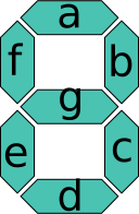
These segments can theoretically be used to represent all 16 digits of hexadecimal encodings, which we can represent with variables $x_3$, $x_2$, $x_1$, $x_0$. Let’s just stick to the first 10 digits for this lab.
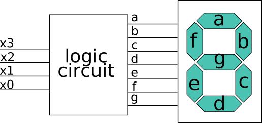
Before the lab, complete this truth table for encodings of digits 2, 3, 5, and 8.
| $x_3$ | $x_2$ | $x_1$ | $x_0$ | Digit | a | b | c | d | e | f | g |
|---|---|---|---|---|---|---|---|---|---|---|---|
| 0 | 0 | 0 | 0 | 0 | 1 | 1 | 1 | 1 | 1 | 1 | 0 |
| 0 | 0 | 0 | 1 | 1 | 0 | 1 | 1 | 0 | 0 | 0 | 0 |
| 0 | 0 | 1 | 0 | 2 | |||||||
| 0 | 0 | 1 | 1 | 3 | |||||||
| 0 | 1 | 0 | 0 | 4 | 0 | 1 | 1 | 0 | 0 | 1 | 1 |
| 0 | 1 | 0 | 1 | 5 | |||||||
| 0 | 1 | 1 | 0 | 6 | 1 | 0 | 1 | 1 | 1 | 1 | 1 |
| 0 | 1 | 1 | 1 | 7 | 1 | 1 | 1 | 0 | 0 | 0 | 0 |
| 1 | 0 | 0 | 0 | 8 | |||||||
| 1 | 0 | 0 | 1 | 9 | 1 | 1 | 1 | 1 | 0 | 1 | 1 |
A Programming Analogy#
Write a case/switch statement in your favorite programming language that takes inputs $x_3$, $x_2$, $x_1$, $x_0$ and outputs the correct values for the segment labels a-g.
Deliverable Checkpoint
Submit your pre-lab work in any of these ways: (1) submit it to Canvas, (2) upload it to your repository and link to it in the Feedback PR, (3) email it to me, (4) show it to me in-person.
Lab Setup#
This lab provides brief instructions under the assumption that you have already done several of these steps successfully. Refer back to Lab1 for more detailed instructions.
- Clone the assignment repository:
git clone <url> <custom_name> - Start Vivado.
This lab provides less explicit instruction than previous labs. The goal of this is to gradually remove scaffolding and help you build independence working with complex systems. You’ll probably need help; you can ask for it anytime from your instructor or classmates.
Clock Division#
Now let’s shift attention and experiment with the board’s built-in clock resource. The Basys3 has a system clock rate with frequency 100 MHz. In this exercise, we will create a clock divider module to slow down the clock so that we can observe step-by-step events. We will reduce the clock rate to 2 Hz, i.e. two events per second, so that you can actually see the clock tick. A slow, observable clock can be useful for studying and debugging sequential logic circuits.
Clock Divider Design#
In Vivado, create a new project with the following specification:
- Project name: ClockDivider
- Project location: directory of this assignment’s repository
- Create project subdirectory should be checked
- Constraints: Select the Basys3Master.xdc file, which can be downloaded from Canvas
- Choose the Basys3 board in board selection
- Don’t worry about inputs and outputs for now
If it doesn’t already exist, create a new Verilog Design Source for a module named ClockDivider.v.
Your module should have one input and one output, and the initial template code should look like this (header comments are not shown):
‘timescale 1 ns/1 ns
module ClockDivider #(parameter PRESCALER = 25 _000_000)(
    input clkin ,
    output reg clkout
    );
endmodule
Notice that the keyword reg is inserted in the declaration of clkout. This is because the clkout signal will be defined behaviorally in an always block.
Parameters#
The parameter keyword is placed between the module name and the opening parenthesis for the port declarations with its own set of parentheses with a leading # symbol. The keyword parameter is used to provide different customizations to a module instance.
A default value can be assigned to the parameter. Here, 25 million (25_000_000) is used as the default. We will eventually override this parameter in the testbench so that the testbench doesn’t take 10 years to simulate our clock divider.
For a hierarchical design, parameters can be passed down from a top-level Verilog module to the instantiations of lower-level modules within the top-level module.
Clock Division#
To divide the clock rate, we’ll use a simple counter method. We will declare a count variable, initialize it at zero, and increment by one in each cycle of clkin. Once the count adds up to a divisor N, we will flip clkout. Thus, the frequency of clkout should be as follows:
$$ f_{out} = \frac{f_{in}}{2N} $$
If our $f_{in} = 100 \text{MHz} = 100 \times 10^6 \text{Hz}$, we can get $f_{out} = 2 \text{Hz}$ from divisor $N = 25 \times 10^6$.
Now we need to represent $N$ in an efficient way. We can find the number of bits required for $N$ with a logarithm: $\lceil \log_2 N \rceil = 25$ bits.
Implementation#
Now we have everything we need to implement our clock divider. Let’s add the following lines to our module definition:
    reg [24:0] count; // a 25-bit register to count up to N

    initial begin
        count = 0; // initialize the counter to 0
        clkout = 0; // inititalize the output clock to 0
    end
    always @( posedge clkin ) begin // at every input clock cycle
        if ( count == PRESCALER ) begin // check if the count has reached N
            count <= 0; // reset the count
            clkout = ~clkout; // toggle the output clock
        end
        else begin
            count <= count + 1; // leave the output clock alone and keep counting
        end
    end
In this code, the 25-bit variable count is treated, by default, as an integer. The code in the always block is executed synchronously with the rising edge of the input clock. At each clock, count isincremented by 1. When count reaches the PRESCALER value, clkout is toggled (the ~ symbol means “not”).
Clock Divider Simulation#
Now we will create a testbench for the ClockDivider module. For simulation purposes, it will be easier to reduce N to a small number, such as eight. To do this, we are going to override the default parameter we gave to the ClockDivider module. This can be done like assigning ports: use a dot followed by the parameter name with the value you want to pass in enclosed parentheses. Now instead of having a value of 25 million, it will simulate with a value of 8 so that we do not have to simulate millions of clock cycles to verify the design. Parameters are a nice way to configure modules.
The value 8 is only used in simulation. When we implement the design on the board, it will remain at 25 million. If we did not use the parameter altogether, then you would have to remember to comment out the existing value in the ClockDivider.v module and replace it with a smaller value. Then when you are ready to implement the design, you would have to remember to switch which lines were previously commented out. If you forgot to do so, the LED would appear to be always on, as it is blinking too fast.
Save all your work, then click on Add Sources, select Add Simulation Sources and follow the procedures
for making a simulation testbench. Open your new testbench file. You now need to setup the input clock.
The easiest way is to define an infinite loop using the forever keyword in an initial block:
module testbench(
);
    reg board_clk;
    wire slow_clk;

    ClockDivider #(.PRESCALER(8)) DUT(
        .clkin(board_clk),
        .clkout(slow_clk)
        );

    initial begin
        clkin = 0;
        forever #10 clkin = ~clkin;
    end
endmodule
Add comments to this testbench. In your lab notebook, describe what this testbench is doing.
Save your testbench file and run a behavioral simulation as we did before. In the waveform viewer, click the zoom-to-fit icon to see your simulation range. You should see a fast clock toggling 9 times for every toggle of the slow clock.
Why does a prescaler of 8 cause a toggle every 9 clock cycles? Answer this in your lab notebook.
Deliverable Checkpoint
Demonstrate your successful simulation to the instructor in-person or by taking a screenshot.
Clock Divider Implementation#
Now we need to configure the Constraint File for implementation. You should have already added Basys3Master.xdc as a constraint to your project; if not, do so now. Open the constraint file. We will need to find lines that define the system clock, named clk in the default configuration. We will also need to associate LED[0] with clkout. Your completed constraint file should look like this:
set_property PACKAGE_PIN U16 [get_ports {clkout}]
	set_property IOSTANDARD LVCMOS33 [get_ports {clkout}]

set_property PACKAGE_PIN W5 [get_ports clkin]
        set_property IOSTANDARD LVCMOS33 [get_ports clkin]
        create_clock -add -name sys_clk_pin -period 10.00 -waveform {0 5} [get_ports clkin]
You must be very careful to ensure that the names referenced with the get ports keyword match precisely with the signal names in your design. Once your constraint is complete, run Synthesis, Implementation and Generate Bitstream. Program your device and verify that the LED blinks about twice per second.
Deliverable Checkpoint
Demonstrate your successful program to the instructor in-person or by recording a video of all possible input configurations. If you submit videos, please upload them to Box or OneDrive, ensure anyone with the link can view them, then share the link. Submit your code at this stage by tagging your current commitslowclkand pushing tags.
Seven-Segment Display#
In Example 2.15 of the textbook, you are asked to consider the relationship between a binary-coded decimal (BCD) number and the corresponding lights on a seven-segment display. The BCD digits are labeled $x_3$, $x_2$, $x_1$ and $x_0$ (with $x_3$ as the most significant bit), representing a number between 0 and 9. The display’s individual segments are labeled a-g, with each signal corresponding to one illuminated edge in the display. The truth table you completed in your pre-lab work is used for a standard display.
Implicit Sensitivity#
There are a few different ways to model a truth table in Verilog. In each method, we will use an always block with implicit sensitivity:
always @(*) begin
    ...
end
The * requires the code in this block to execute whenever any of the signals inside the always block change. ” This type of sensitivity list is only appropriate for combinational logic, and it calls for the use of blocking assignment statements (i.e., assignments with = instead of <=).
Compact Signals#
Verilog allows us to concatenate multiple signals into one bit vector. That is, we can pack our inputs and outputs into compact signals that allow for easier implementation of a case statement.
The following can concatenate the four input variables into a single wire:
wire [3:0] inputbv = {x3,x2,x1,x0};Similarly, we can create a compact signal for outputs with continuous assignments:
wire [6:0] outputbv;
assign a = outputbv[6];
assign b = outputbv[5];
...
assign g = outputbv[0];
Then we can use a case statement:
always @(*) begin
    case ( inputbv )
        4'b0000 : outputbv = 7'b1111110 ; // 0
        4'b0001 : outputbv = 7'b0110000 ; // 1
        ...
        4'b1001 : outputbv = 7'b1111011 ; // 9
        // Always provide a " default " case to catch
        // unexpected or invalid inputs :
        default : outputbv = 7'b0000000 ;
    endcase
end
Design a Seven-Segment Display#
It’s your turn to put your Verilog skills to the test! Create a new project for your seven segment display called Combinational. Design and simulate a system that meets the following criteria. Do not implement this yet; we’ll program our boards in Lab4.
- Boolean inputs
x3,x2,x1, andx0that correspond to the above truth table - Boolean outputs
a,b,c,d,e,f,gthat correspond to the above truth table - A case statement inside an
alwaysblock that produces the logic from the above truth table
Create a testbench includes at least the following:
module SevenSegmentTest;
    // Inputs (as individual bits)
    reg [3:0] x;
    reg       clk;

    // Outputs (segments a-g)
    wire a, b, c, d, e, f, g;

    // Instantiate the DUT using individual bit ports x3..x0 and outputs a..g
    SevenSegment DUT (
        .x3(x[3]),
        .x2(x[2]),
        .x1(x[1]),
        .x0(x[0]),
        .a(a),
        .b(b),
        .c(c),
        .d(d),
        .e(e),
        .f(f),
        .g(g)
    );

    initial begin
        x = 4'b0000;
        clk = 0;

        #100;
        forever #10 clk = ~clk; // 50 MHz simulation clock toggling every 10 time units
    end

    // Cycle through 0..9 on each rising clock edge
    always @(posedge clk) begin
        if (x >= 4'd9)
            x <= 4'd0;
        else
            x <= x + 1;
    end

endmodule
When your testbench module is ready, launch the simulation and zoom in so that you can see individual clock cycles. Verify the first couple of truth table rows by inspecting the bit values.
Deliverable Checkpoint
Submit your code at this stage by tagging your current commitsevenand pushing tags.
Deliverables#
Indicate to your instructor that you’re ready to submit your work by leaving a comment on the Feedback PR and requesting a review from @mossbiscuits. Ensure that your submission is on the main branch. Create a tag named done to mark your submission:
git tag -a done -m "Lab3 submission"
git push origin done
If you took photos, screenshots, or videos, remember to upload them to Box or OneDrive and link to them in the Feedback PR. Alternatively, you can submit these items directly on Canvas.
To receive 100 points, submissions must include evidence of the following:
- (20) Correct, timely solution to the pre-lab work
- (40) Correct simulation and working implementation of a clock divider
- (40) Correct simulation of the seven-segment display