L3: Verilog & CAD#
Using computers to design computers.
Objective
Develop a basic understanding of CAD processes, especially digital circuit design using Verilog.
Before the Lecture#
Required Reading
- 2.9 (Introduction to CAD Tools)
- 2.10 (Introduction to Verilog)
- Skim A.1–A.12 (Verilog Reference)
Optional Supplemental Instruction
- Introduction to Verilog - ChipVerify
- An Introduction to Verilog - CompArchIllinois on YouTube
- Introduction to Verilog - Carleton University
Design Entry#
Design Entry is the process of specifying a digital circuit’s functionality and structure. There are several methods for design entry, each with its own advantages and limitations.
-
Truth tables: One of the simplest methods for design entry. Practical for only small circuits, as they explicitly list all possible input combinations and their corresponding outputs. While effective for understanding basic logic, truth tables become unwieldy as the complexity of the circuit increases.
-
Schematic capture: Designers interconnect symbols from a predefined library to represent the circuit. This approach facilitates hierarchical design, allowing designers to break down a complex circuit into smaller, manageable modules. Schematic capture is well-suited for larger circuits but becomes difficult to use for very large or highly complex designs due to the sheer number of components and connections.
-
Hardware description language (HDL): Scalable and flexible. HDLs, such as Verilog and VHDL, are comparable to programming languages and are specified in IEEE standards. They offer design portability, enabling circuits to be shared and reused across different projects. HDLs also support hierarchical design, making it easier to manage complex systems. They can be combined with schematics to take advantage of the strengths of both methods.
HDLs are particularly powerful because they allow for the simulation and verification of designs before physical implementation. This reduces the risk of errors and ensures that the design meets the required specifications. Additionally, HDLs enable parameterized designs, where components can be reused with different configurations, saving time and effort in large-scale projects. The use of HDLs is a standard practice in modern digital design workflows.
Logic Synthesis#
Logic synthesis, or logic optimization, is the process of translating a truth table, schematic, or HDL code into a network of logic gates. Converting a logic description to a physical design entails resource mapping and layout synthesis. That is, one must select the actual hardware components that produce the logic that is abstractly represented by a circuit design. Because it is impossible for an engineer to manually produce an optimal circuit, automated tools are almost always a key part of the design workflow.
Logic synthesis tools (such as those included in Vivado) aim to optimize the design for specific criteria, such as minimizing area, power consumption, or maximizing speed. These tools also ensure that the design adheres to the constraints of the target technology, such as the capabilities of the fabrication process or the performance requirements of the application. By automating the translation from high-level descriptions to gate-level implementations, logic synthesis significantly accelerates the design process and improves the overall efficiency of digital circuit development.
Functional Simulation#
Functional simulation is a critical step in verifying the correctness of a digital circuit design. Using a functional simulator, designers provide specific input values to the circuit and observe its responses. The simulator evaluates the circuit’s behavior based on the design description, allowing the user to compare the simulated outputs against the expected results. This process ensures that the circuit operates as intended before proceeding to further stages of the design flow, such as synthesis or physical implementation. Functional simulation helps identify and resolve logical errors early, saving time and resources in the development process.
Physical Design#
Physical design involves translating the synthesized logic into a physical layout that can be fabricated on a chip. This step includes placing the logic gates and other components onto the chip’s surface and routing the connections between them. The goal is to optimize the layout for performance, power efficiency, and area utilization while adhering to the constraints of the manufacturing process. Tools like place-and-route software automate much of this process, ensuring that the design meets timing requirements and avoids issues such as signal interference or excessive power consumption.
Timing Simulation#
Timing simulation is performed after physical design to verify that the circuit meets its timing requirements under real-world conditions. This step involves simulating the circuit with accurate timing information, including propagation delays introduced by the physical layout, interconnects, and other factors. Timing simulation ensures that the circuit operates correctly at the desired clock frequency and helps identify issues such as setup and hold time violations. By addressing these problems early, designers can make adjustments to the layout or design to ensure reliable operation in the final implementation.
Circuit Implementation#
Circuit implementation is the culmination of the digital design process, where the verified and optimized design is physically realized into a tangible form. This step can take one of two primary paths: programming the design onto a programmable device, such as a Field-Programmable Gate Array (FPGA), or fabricating it as an Application-Specific Integrated Circuit (ASIC).
FPGA Implementation#
For FPGA implementation, the process involves generating a bitstream file that configures the FPGA to match the design. This bitstream is created using specialized software tools that translate the synthesized and placed-and-routed design into a format that the FPGA can understand. Once programmed, the FPGA can be tested in real-world conditions to ensure that it meets the design specifications. FPGAs are particularly advantageous for prototyping and low-volume production due to their reprogrammability and shorter development cycles.
ASIC Fabrication#
For ASICs, the implementation process is more complex and involves sending the design to a semiconductor foundry for manufacturing. This includes creating photolithographic masks, which are used to etch the design onto silicon wafers during the fabrication process. ASICs are ideal for high-volume production because they offer better performance, lower power consumption, and reduced unit costs compared to FPGAs. However, the upfront costs and time required for ASIC development are significantly higher, making them less suitable for small-scale projects.
Ensuring Reliability#
Regardless of the implementation method, proper testing and validation are critical to ensure that the final product meets the design specifications and performs reliably in its intended application. For FPGAs, this may involve in-system testing and debugging, while for ASICs, additional steps such as wafer testing and packaging are required. By carefully managing the implementation process, designers can ensure that the final product is both functional and optimized for its target application.
Complete Design Flow#
The following flowchart (similar to Figure 2.35 in the textbook) represents a typical CAD workflow.
---
title: "Typical CAD Workflow"
config:
    theme: 'default'
---
flowchart TD
    A([Design conception]) --> DESIGN-ENTRY
    subgraph DESIGN-ENTRY [Design Entry]
        DE1([Schematic Capture])
        DE2([HDL Specification])
    end
    DESIGN-ENTRY --> B
    B[Synthesis] --> C[Functional Simulation]
    C --> D{Design Correct?}
    D -->|Yes| E
    D -->|No| DESIGN-ENTRY
    E[Physical Design] --> F[Timing Simulation]
    F --> G{Timing Requirements Met?}
    G -->|Yes| H
    G -->|No| DESIGN-ENTRY
    H[Chip Configuration]
Basic Verilog Syntax#
Module Declaration#
A Verilog design begins with the module keyword and ends with endmodule. The module’s name is specified after the module keyword, followed by a list of input and output ports enclosed in parentheses. For example:
module example1 (
    input A, B, C,
    output D
);Ports#
Ports are the inputs and outputs of a module. They are declared using the input and output keywords. For instance:
input A, B, C;
output D;
Wire Declaration#
wire is used to declare internal connections between components within a module. These wires serve as intermediate signals that connect the outputs of one component to the inputs of another. For example:
wire w1;
wire w2;
Register Declaration#
In Verilog, reg is used to declare registers that can store values. Unlike wire, which represents connections between components, reg is used in procedural blocks (e.g., always or initial) to hold values that are assigned using procedural statements. A reg variable retains its value until it is explicitly updated, making it suitable for modeling storage elements like flip-flops or for use in testbenches. For example:
reg clk;Choosing wire or reg#
A wire represents a physical connection in hardware, used to model combinational logic or connect different modules. It cannot store values and is driven by continuous assignments or module outputs, making it suitable for signals that are purely combinational.
A reg represents a storage element in hardware, used to model sequential logic or store values in procedural blocks like always blocks. Unlike wire, a reg can hold values across simulation time steps, making it ideal for modeling sequential elements such as flip-flops or latches.
Use wire for signals driven by combinational logic or module outputs, and use reg for signals that require value storage or are assigned within procedural blocks.
Signal Connections#
Signals, such as A, B, C, w1, w2, and D, are connected to the inputs and outputs of gates to define the circuit’s behavior. These connections specify how data flows through the circuit.
Structural Specification in Verilog#
Verilog allows designers to describe the structure and behavior of digital circuits at various levels of abstraction, from high-level functional descriptions to low-level gate implementations. One way to construct simple circuits in Verilog is through the use of structural specification, which provides a coarse abstraction of a circuit. This allows a close mapping of a circuit diagram to the HDL specification.
Gate-Level Primitives#
Verilog provides a set of built-in gate-level primitives that represent basic logic gates. These primitives are predefined in the language and can be used directly in structural specifications. The general format for using a gate-level primitive is:
<primitive_name> <instance_name>(<output>, <input1>, <input2>, ...);<primitive_name>is the type of gate (e.g.,and,or,not, etc.).<instance_name>is a user-defined identifier for the gate instance.<output>is the signal driven by the gate.<input1>, <input2>, ...are the input signals to the gate.
These primitives are particularly useful for low-level design and for understanding the fundamental building blocks of a circuit. In practice, there is almost always a nicer way to design a circuit.
Common Verilog Primitives#
-
and: Represents an AND gate. This gate can have many inputs.
and and1(out, in1, in2); and and2(out, in1, in2, in3, ...); -
or: Represents an OR gate. This gate can have many inputs.
or or1(out, in1, in2); or or2(out, in1, in2, in3, ...); -
not: Represents a NOT gate (inverter). This gate can only have one input.
not not1(out, in); -
nand: Represents a NAND gate. This gate can have many inputs.
nand nand1(out, in1, in2); nand nand2(out, in1, in2, in3, ...); -
nor: Represents a NOR gate. This gate can have many inputs.
nor nor1(out, in1, in2); nor nor2(out, in1, in2, in3, ...); -
xor: Represents an XOR gate. This gate can only have two inputs.
xor xor1(out, in1, in2); -
xnor: Represents an XNOR gate. This gate can only have two inputs.
xnor xnor1(out, in1, in2);
Verilog Primitives Example#
The following example shows how to use these primitives:
module example1 (
    input A, B, C,
    output D
);

    wire w1;
    wire w2;

    // OR gate
    or gate1(w1, A, B);

    // NOT gate
    not gate2(w2, C);

    // AND gate
    and gate3(D, w1, w2);

endmodule
The Verilog module example1 specifies the following circuit:
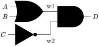
This example demonstrates the use of Verilog’s gate-level primitives to model basic logic gates. The initial block serves as a testbench to simulate the circuit and display the results for different input combinations.
Hierarchical Design#
If you are familiar with software design, you’ll understand the value of functions: you can design something once and use it many times. This is an example of modular or heirarchical design. Verilog supports hierarchical design, which promotes reusability, simplifies debugging, and enhances the overall organization of a design. By breaking down a large system into smaller modules, engineers can focus on individual components, verify their functionality, and then integrate them into the larger system.
Module Instantiation#
In hierarchical design, modules can be instantiated within other modules. This means that a module can serve as a building block for a higher-level module. The process of instantiating a module involves creating an instance of the module and connecting its ports to the appropriate signals in the parent module. This allows for the reuse of the same module in different parts of the design, reducing redundancy and improving maintainability.
The general syntax for module instantiation is as follows:
<module_name> <instance_name> (
    .module_port(parent_signal),
    .module_port(parent_signal),
    ...
);<module_name>: The name of the module being instantiated.<instance_name>: A unique identifier for the instance..module_port(parent_signal): Maps a port in the instantiated module (module_port) to a signal in the parent module (parent_signal).
This syntax ensures that the ports of the instantiated module are explicitly connected to the corresponding signals in the parent module, making the design clear and maintainable.
Gate-Level Instantiation#
Gate-level primitives provide a specific form of modular design where basic logic gates (such as and, or, not, etc.) are instantiated directly within a module.
Benefits of Hierarchical Design#
- Modularity: Hierarchical design allows designers to divide a system into smaller, manageable modules. Each module can be developed and tested independently, making the design process more efficient.
- Reusability: Modules can be reused across different projects or within the same design, reducing development time and effort.
- Scalability: Hierarchical design makes it easier to scale a system by adding or modifying modules without affecting the entire design.
- Readability: By organizing a design into smaller modules, the overall structure becomes easier to understand and maintain.
Example of Hierarchical Design#
The following example demonstrates how to use hierarchical design in Verilog:
module half_adder (
    input HA_A, HA_B,
    output HA_Sum, HA_Carry
);

    // Instantiate AND gate for Carry
    and g1 (HA_Carry, HA_A, HA_B);

    // Instantiate OR gate for Sum
    or g2 (HA_Sum, HA_A, HA_B);

endmodule

module two_half_adders (
    input A, B, C,
    output Sum1, Carry1, Sum2, Carry2
);

    // Instantiate the first half_adder module
    half_adder ha1 (
        .HA_A(A),
        .HA_B(B),
        .HA_Sum(Sum1),
        .HA_Carry(Carry1)
    );

    // Instantiate the second half_adder module
    half_adder ha2 (
        .HA_A(Sum1),
        .HA_B(C),
        .HA_Sum(Sum2),
        .HA_Carry(Carry2)
    );

endmodule
In this example:
- The
half_addermodule implements the logic for a simple half adder using basic gates. - The
two_half_addersinstantiates thehalf_addermodule twice, showing how smaller modules can be reused in a larger design.
Behavioral Specification in Verilog#
Behavioral specification allows designers to describe the functionality of a digital circuit at a higher level of abstraction rather, focusing on what the circuit does rather than how it is implemented. This approach is particularly useful for complex designs where specifying every gate and connection would be impractical. It offers several advantages:
- Abstraction: Behavioral specification abstracts away the low-level details of the circuit, enabling designers to focus on the desired functionality rather than the implementation.
- Efficiency: Writing behavioral code is faster and more concise compared to gate-level descriptions, especially for large and complex systems.
- Readability: Behavioral code is easier to read and understand, making it more accessible for debugging and collaboration.
- Simulation and Verification: Behavioral models are well-suited for simulation and functional verification, allowing designers to test the circuit’s behavior early in the design process.
- Portability: Behavioral descriptions are independent of the underlying hardware, making them reusable across different technologies and platforms.
Behavioral specification in Verilog is typically written using procedural blocks, such as always and initial, continuous assignments using assign, and high-level constructs like if, case, and loops. These constructs allow designers to describe the circuit’s behavior in a way that resembles software programming.
Procedural Assignment with always Blocks#
The always Block#
The always block in Verilog is a procedural construct used to describe behavior that depends on changes in signals. It is triggered by events specified in its sensitivity list, which can include specific signals or edges (e.g., rising or falling edges). The always block is particularly useful for modeling both combinational and sequential logic. For combinational logic, the sensitivity list typically includes all input signals, while for sequential logic, it often includes clock and reset signals. The block executes whenever an event in the sensitivity list occurs, allowing designers to specify how the circuit should respond to changes in input signals. The syntax for an always block is as follows:
always @(sensitivity_list) begin
    // Behavioral description
end
A sensitivity list determines when an always block should execute. For example, in the following code, the block executes whenever A changes, so C only updates when A updates (agnostic to a change in B).
always @(A) begin
    C = A & B;
end
The initial Block#
The initial block in Verilog is used for one-time initialization of signals and is primarily employed in testbenches. Unlike the always block, which executes repeatedly based on its sensitivity list, the initial block runs only once at the start of the simulation. It is commonly used to set initial values for signals, generate stimulus for testing, or define clock signals in a testbench environment. The initial block is not synthesizable, meaning it cannot be used to generate hardware, but it is invaluable for simulation and verification purposes. For example, an initial block can be used to apply a sequence of test vectors to a design under test, allowing designers to verify its functionality. The syntax for an initial block is as follows:
initial begin
    // Initialization code
end
Continuous Assignment with assign Statements#
In Verilog, the assign statement is used for continuous assignment, which allows you to define combinational logic directly. It is a powerful construct for describing simple logic without the need for procedural blocks like always.
Syntax#
The general syntax for the assign statement is:
assign <net> = <expression>;<net>: The signal (typically awire) that will be driven by the expression.<expression>: A combinational logic expression that determines the value of the net.
Key Features#
- Continuous Evaluation: The
assignstatement continuously evaluates the expression and updates the net whenever any of the inputs in the expression change. - Combinational Logic: It is ideal for modeling combinational logic, such as gates, multiplexers, and arithmetic operations.
- No Storage: The
assignstatement does not store values; it simply drives the net with the result of the expression.
Examples#
- Simple Logic
assign Y = A & B; // AND gate
assign Z = A | B; // OR gate
- Arithmetic Operations
assign Sum = A + B; // Addition
assign Diff = A - B; // Subtraction
- Conditional Assignment
assign Out = (Sel) ? A : B; // Multiplexer
- Bitwise Operations
assign Result = A ^ B; // XOR operation
assign Inverted = ~A;  // Bitwise NOT
Example: Using assign in a Module#
The following example demonstrates how to use the assign statement to implement a 2-to-1 multiplexer:
module mux2to1 (
    input wire A, B, Sel,
    output wire Out
);

    // Continuous assignment for multiplexer logic
    assign Out = (Sel) ? B : A;

endmodule
In this example:
- The
assignstatement implements the multiplexer logic, selecting between inputsAandBbased on the value ofSel. - The
Outsignal is continuously updated wheneverA,B, orSelchanges.
When to Use assign#
- For simple combinational logic that does not require procedural constructs.
- When you want to describe logic concisely and clearly.
- For driving
wiretypes with expressions.
Limitations of assign#
- It cannot be used to model sequential logic or storage elements (e.g., flip-flops).
- It is limited to driving
wiretypes and cannot be used withreg.
The assign statement is a fundamental construct in Verilog, enabling designers to describe combinational logic in a concise and intuitive manner. By leveraging assign, you can create clean and efficient designs for a wide range of digital circuits.
Why Use Behavioral Specification Instead of Gate-Level Primitives?#
- Scalability: Gate-level primitives are suitable for small circuits but become unwieldy for larger designs. Behavioral specification scales better for complex systems.
- Flexibility: Behavioral code can be easily modified to accommodate changes in design requirements, whereas gate-level descriptions require significant rework.
- Automation: Behavioral descriptions can be synthesized into optimized gate-level implementations by CAD tools, saving time and effort.
- Focus on Functionality: Designers can concentrate on what the circuit should do, leaving the details of how it is implemented to synthesis tools.
- Faster Development: Behavioral specification accelerates the design process, enabling rapid prototyping and iteration.
Control Flow#
Control flow constructs in Verilog allow designers to specify the behavior of a circuit based on conditions or iterative processes. These constructs are particularly useful in behavioral modeling, where the focus is on describing the functionality of a design.
if-else#
The if-else statement is used for conditional execution of code. It evaluates a condition and executes the corresponding block of code based on whether the condition is true or false. This construct is ideal for implementing decision-making logic in a design.
if (condition) begin
        // Code for true condition
end else begin
        // Code for false condition
endcase#
The case statement is used for multi-way branching based on the value of a signal. It is particularly useful for implementing decoders, state machines, and other designs with multiple conditions.
case (signal)
        value1: // Code for value1
        value2: // Code for value2
        default: // Default code
endcaseLoops#
Verilog supports loops like for, while, and repeat for iterative behavior. These constructs are primarily used in testbenches and should not be used in synthesizable code to avoid unintended hardware replication.
for Loop: Executes a block of code for a specified number of iterations.
for (i = 0; i < N; i = i + 1) begin
        // Loop body
end
while Loop: Executes a block of code as long as the condition is true.
while (condition) begin
        // Loop body
end
repeat Loop: Executes a block of code a fixed number of times.
repeat (N) begin
        // Loop body
end
forever Loop: Executes a block of code indefinitely. This construct should only be used in testbenches to model continuous behavior, such as clock generation.
forever begin
    // Loop body
end
A forever loop is often used in testbenches to generate a clock signal. For example:
reg clk;

initial begin
    clk = 0; // Initialize clock
    forever #5 clk = ~clk; // Toggle clock every 5 time units
end
Practice Exercises#
-
Create a Verilog module for a circuit representing $D = (A \land B) \lor \neg C$
View Solution
This is just an example; there are many possible ways to implement this.
module logic_example ( input wire A, B, C, output wire D ); wire and_result, not_result; and g1(and_result, A, B); not g2(not_result, C); or g3(D, and_result, not_result); endmodule -
Write a Verilog module for a 4-input AND gate using continuous assignment.
View Solution
This is just an example; there are many possible ways to implement this.
module and4 ( input wire A, B, C, D, output wire Out ); assign Out = A & B & C & D; endmodule -
Create a hierarchical Verilog design for a circuit that instantiates two of the following module according to the following specifications:
module example (
    input wire A, B,
    output wire Out
);

    assign Out = A & B;

endmodule
The
examplemodule represents a simple 2-input AND gate. Your task is to create a new module that instantiates two instances of theexamplemodule and connects them to form a larger circuit. The new module should have three inputs (X,Y,Z) and one output (Result). The circuit should calculate $Out = (X \land Y) \land Z$.View Solution
This is just an example; there are many possible ways to implement this.
module hierarchical_example (
    input wire X, Y, Z,
    output wire Result
);

    wire W; // Intermediate signal

    // Instantiate the first AND gate
    example andgate1 (
        .A(X),
        .B(Y),
        .Out(W)
    );

    // Instantiate the second AND gate
    example andgate2 (
        .A(W),
        .B(Z),
        .Out(Result)
    );

endmodule