L2: Logic Circuits#
The backbone of digital systems and modern computing.
Objective
Gain a basic understanding of logic circuits, including their theoretical foundations, practical design, and role in digital systems.
Before the Lecture#
Required Reading
- 2.1: Variables and Functions
- 2.2: Inversion
- 2.3: Truth Tables
- 2.4: Logic Gates & Networks
Optional Supplemental Instruction
- Boolean Logic & Logic Gates - Crash Course Computer Science
Binary Logic Circuits#
Binary logic circuits are essential for processing digital signals, which are represented as binary values (0 and 1). These circuits form the foundation of all digital systems, enabling computation, data storage, and communication.
- Binary Representation: Operates on two discrete states:
0(low/off) and1(high/on). - Implementation: Built using electronic components like transistors, diodes, and resistors.
- Applications: Used in arithmetic operations, decision-making processes, and control systems.
Binary logic circuits are implemented using logic gates, which perform specific logical operations. These gates are the building blocks of more complex digital systems.
Switches in Logic Circuits#
Switches are fundamental to the operation of logic circuits. They act as binary devices, toggling between two states: ON (1) and OFF (0). In digital systems, switches control the flow of current, representing binary values.
By combining switches, we can create logic gates that perform specific operations. For example, transistors are widely used in modern circuits due to their efficiency and scalability.

Animation: Candidomolino, CC BY-SA 4.0, via Wikimedia Commons

Switches provide a tangible way to understand how logic gates operate, bridging the gap between theoretical concepts and real-world implementation.
Truth Tables#
Truth tables are a key tool in digital logic design. They list all possible input combinations for a circuit or expression and their corresponding outputs, making it easy to verify and debug logic designs.
Why Use Truth Tables?#
Truth tables are useful for:
- Verification: Ensuring circuits or expressions work as intended.
- Debugging: Identifying errors in logic design.
- Simplification: Helping minimize logic expressions.
Structure of a Truth Table#
A truth table includes:
- Input Columns: All binary input combinations (
0and1). - Output Columns: Outputs for each input combination.
For example, the truth table for an AND gate with inputs A and B:
| Input A | Input B | Output (A AND B) |
|---|---|---|
| 0 | 0 | 0 |
| 0 | 1 | 0 |
| 1 | 0 | 0 |
| 1 | 1 | 1 |
Applications of Truth Tables#
Truth tables are used in:
- Logic Gate Analysis: Understanding gates like AND, OR, and NOT.
- Circuit Design: Verifying complex circuits.
- Boolean Expression Evaluation: Testing expressions for all inputs.
Mastering truth tables builds a strong foundation for digital logic design.
Logic Gates#
Logic gates are the fundamental components of digital circuits. They perform basic logical operations on binary inputs to produce a binary output.
Logic gates process binary inputs to produce specific binary outputs based on their logical function. They are the building blocks of digital circuits, enabling the execution of fundamental operations such as addition, subtraction, and data comparison. Each gate operates according to a truth table, which defines the relationship between its inputs and outputs.
In addition to their standalone functions, logic gates can be combined to create more complex circuits. By interconnecting gates, designers can implement arithmetic operations, memory storage, and decision-making processes. These combinations form the basis of components like multiplexers, decoders, and arithmetic logic units (ALUs) in digital systems.
Logic gates are not only used in computational devices but also in control systems, communication networks, and embedded systems. Their versatility and reliability make them indispensable in modern technology, from simple household appliances to advanced computing systems.
NOT Gate#
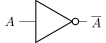
The NOT gate is a unary operator that inverts its input. If the input is 1, the output is 0, and vice versa.
The logical NOT operator (negation) is represented by various symbols depending on the context:
- $\neg$ is commonly used in formal logic and Boolean algebra.
NOTis frequently used in programming and digital circuit design.!is used in many programming languages like C, C++, and Java for logical NOT operations.~is occasionally used in some programming languages or shorthand notations.- Overlining (e.g., $\overline{A}$) is often used in circuit diagrams and mathematical notation to indicate negation.
| Input | Output (NOT Input) |
|---|---|
| 0 | 1 |
| 1 | 0 |
Symbol:
AND Gate#
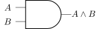
The AND gate is a binary operator that outputs 1 if and only if BOTH inputs are 1.
The logical AND operator (conjunction) is denoted with the following:
- $\cdot$ is often used in mathematical notation.
- $\land$ is frequently used in formal logic and Boolean algebra.
ANDis commonly used in programming and digital circuit design.&is occasionally used in some programming languages or shorthand notations.*is sometimes used in simplified or informal contexts.&&is used in many programming languages like C, C++, and Java for logical AND operations.
| Input A | Input B | Output (A AND B) |
|---|---|---|
| 0 | 0 | 0 |
| 0 | 1 | 0 |
| 1 | 0 | 0 |
| 1 | 1 | 1 |
Symbol:
OR Gate#
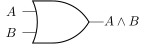
The OR gate outputs 1 if at least one of its inputs is 1. If all inputs are 0, the output is 0.
The logical OR operator is represented using various notations depending on the context:
- $+$ is commonly used in Boolean algebra to denote logical OR.
- $\lor$ is frequently used in formal logic and mathematical notation.
ORis widely used in programming and digital circuit design.|is used in many programming languages like Python and Java for bitwise OR operations.||is used in languages like C, C++, and Java for logical OR operations.
These notations provide flexibility in representing the OR operation across different domains, from theoretical logic to practical circuit design.
| Input A | Input B | Output (A OR B) |
|---|---|---|
| 0 | 0 | 0 |
| 0 | 1 | 1 |
| 1 | 0 | 1 |
| 1 | 1 | 1 |
Symbol:
Combining Gates to Represent Functions#
Logic gates can be combined to create circuits that perform complex logical operations.
Order of Operations in Logic Functions#
The order of operations in Boolean algebra is similar to arithmetic, with specific precedence rules:
- Parentheses: Operations inside parentheses are evaluated first.
- NOT (Negation): Unary operations like $\neg A$ are performed next.
- AND (Conjunction): Binary operations like $A \land B$ are evaluated after NOT.
- OR (Disjunction): Binary operations like $A \lor B$ are evaluated last.
For example, in the expression $(A \lor B) \land \neg C$, the operations are performed in the following order:
- Evaluate $A \lor B$ (inside parentheses).
- Apply $\neg C$ (NOT operation).
- Combine the results using $\land$ (AND operation).
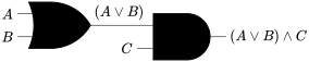
For example, the function $(A \lor B) \land C$ can be implemented using a combination of OR, AND, and NOT gates.
Step-by-Step Implementation:#
- OR Gate: Combine
AandBusing an OR gate to compute $A \lor B$. - AND Gate: Use an AND gate to conjoin the result of $A \lor B$ with $C$.
Circuit Diagram for $(A \lor B) \land C$:#
Truth Table for $(A \lor B) \land C$:#
| Input A | Input B | Input C | A + B | (A + B) * C |
|---|---|---|---|---|
| 0 | 0 | 0 | 0 | 0 |
| 0 | 0 | 1 | 0 | 0 |
| 0 | 1 | 0 | 1 | 0 |
| 0 | 1 | 1 | 1 | 1 |
| 1 | 0 | 0 | 1 | 0 |
| 1 | 0 | 1 | 1 | 1 |
| 1 | 1 | 0 | 1 | 0 |
| 1 | 1 | 1 | 1 | 1 |
Timing Diagrams#
Timing diagrams are graphical representations that show the relationship between input and output signals in a logic circuit over time. They are essential for analyzing the behavior of digital circuits and ensuring proper synchronization.
Key Components of a Timing Diagram:#
- Time Axis: Represents the progression of time, typically from left to right.
- Input Signals: Show the changes in binary values (
0or1) for each input variable. - Output Signals: Display the resulting binary values based on the circuit’s logic.
Timing diagrams help visualize how changes in input signals affect the output, making it easier to debug and optimize circuit designs.
Example Timing Diagram: $C = A \land B$

Example Timing Diagram: $C = A \lor B$

Practice Exercises#
Helpful Tip
The free CircuiTikZ Designer provides an intuitive GUI that can help you typeset beautiful circuit diagrams in CircuiTikZ, a professional way to typeset circuits in $\LaTeX$ documents. It’s what I used to generate the figures on this page. Circuit simulators are also helpful, there is a list on the Resources page.
-
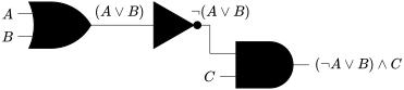
Create a truth table and circuit diagram for $(A \lor B) \land \neg C$
View Solution
$A$ $B$ $C$ $A \lor B$ $\neg C$ $(A \lor B) \land \neg C$ 0 0 0 0 1 0 0 0 1 0 0 0 0 1 0 1 1 1 0 1 1 1 0 0 1 0 0 1 1 1 1 0 1 1 0 0 1 1 0 1 1 1 1 1 1 1 0 0 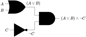
-
Create a truth table and circuit diagram for $\neg(A \land B) \lor C$
View Solution
$A$ $B$ $C$ $A \land B$ $\neg(A \land B)$ $\neg(A \land B) \lor C$ 0 0 0 0 1 1 0 0 1 0 1 1 0 1 0 0 1 1 0 1 1 0 1 1 1 0 0 0 1 1 1 0 1 0 1 1 1 1 0 1 0 0 1 1 1 1 0 1 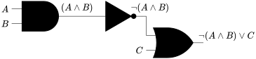
-
Create a truth table for $(\neg A \lor B) \land C$
View Solution
$A$ $B$ $C$ $\neg A$ $\neg A \lor B$ $(\neg A \lor B) \land C$ 0 0 0 1 1 0 0 0 1 1 1 1 0 1 0 1 1 0 0 1 1 1 1 1 1 0 0 0 0 0 1 0 1 0 0 0 1 1 0 0 1 0 1 1 1 0 1 1